After Miniaturization, Comes Stacking
As the miniaturization race reaches its limits, the battlefield has shifted from making chips smaller to assembling them well. Korea excels at making memory, but its accumulated expertise in back-end processing is hollow. This is a gap that fast catch-up alone cannot close.
AI Summary
As physical limits on chip miniaturization force the semiconductor industry to compete on advanced packaging — stacking and integrating chips — Taiwan's TSMC holds a commanding lead built on decades of accumulated failure data, while Korea remains dependent on foreign packaging capacity despite producing world-class DRAM and HBM. The article argues that Korea's short-term performance culture and historical neglect of back-end processes have left it trapped in a structure where its best chips are shipped to someone else's packaging lines. It calls on Korea — and the Busan–southeastern region in particular — to build domestic advanced packaging clusters, treat yield data as a strategic asset, and elevate packaging engineering into a recognized, long-term career discipline.
A Great Chip That Cannot Be Packaged
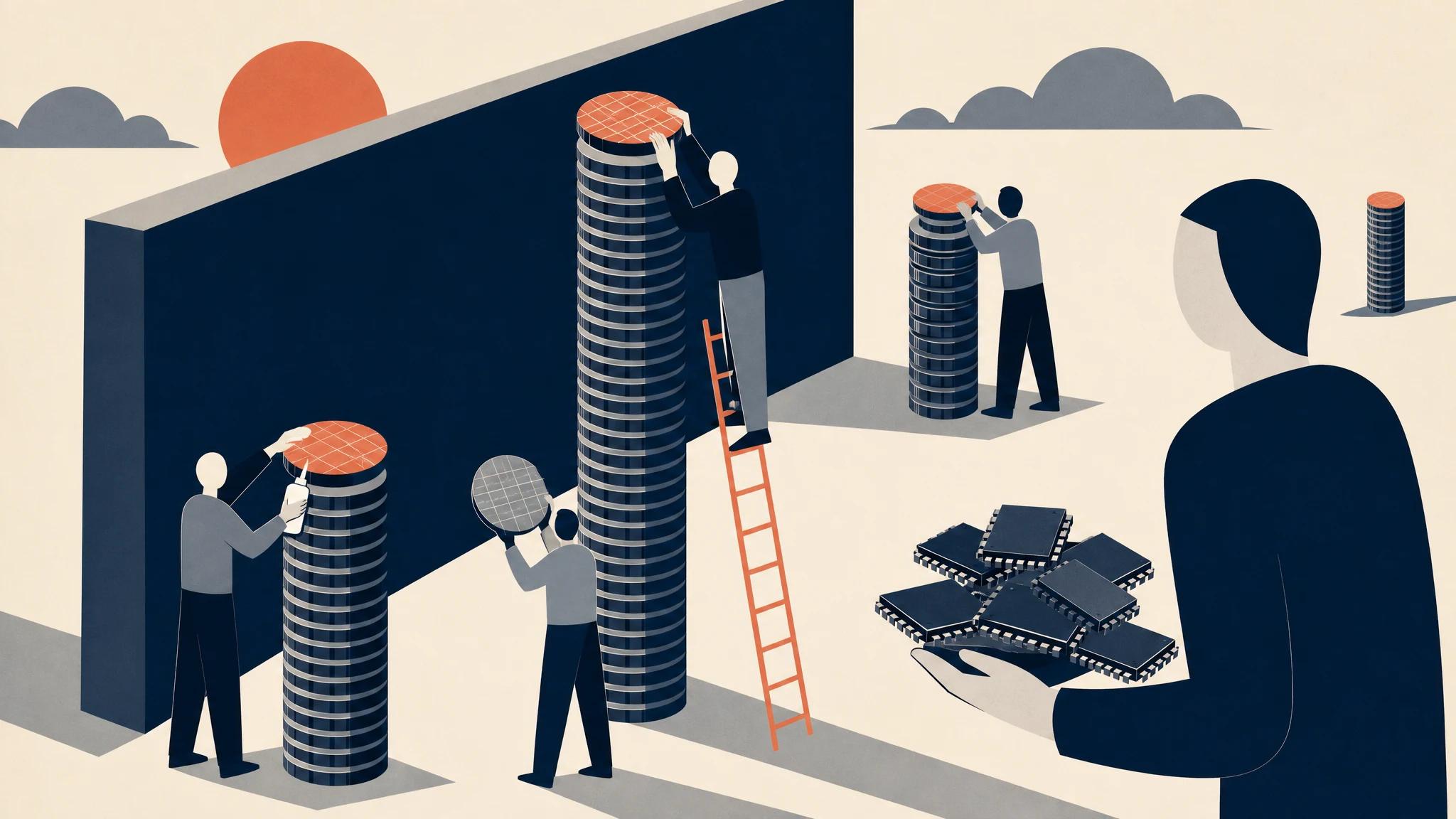
The fact that Samsung and SK Hynix produce the world's finest DRAM remains unshakeable. Yet when you disassemble a product called HBM, the picture changes. HBM is a structure in which multiple DRAM chips are stacked vertically and interconnected by thousands of microscopic holes — Through-Silicon Vias (TSVs) — drilled between them. Making chips and precisely aligning those chips into a single integrated component are two different technologies. Korea is good at the former. The latter is the problem.
In the bill of materials for a single NVIDIA AI accelerator, the most expensive individual component is HBM, and the process of combining that HBM with the GPU into one package is effectively monopolized by Taiwan's TSMC through its CoWoS platform. No matter how superior Korea's memory is, another country controls the chokepoint where it becomes a finished product. The bottleneck in the value chain has migrated from where chips are made to where chips are bonded together. The moment miniaturization reached atomic-scale limits and further shrinkage became difficult, the industry shifted its center of gravity from the competition to make things smaller to the competition to stack things better. This is the domain known as advanced packaging, chiplets, and heterogeneous integration.
Where the Catch-Up Model Cannot Reach
Korea's semiconductor industry grew through catch-up. The model was to solve problems Japan had already answered — faster, cheaper, at greater volume. In a game where the correct answers were predetermined, Korea was faster than anyone. The miniaturization roadmap was generous: what the next node would be, what equipment would be required, what target yield to hit — all of it was shared across the industry. It was an exam with the questions pre-distributed, and Korea scored first.
Packaging is not that kind of exam. There is no answer key for which chips to stack in what order, where to route heat, how to carry signals, or by what criteria to unify chips from different processes into a single body. Design, materials, and process steps are entangled — touch one variable and the rest shift in response. This demands not the ability to solve quickly, but the ability to have been wrong for a long time. It requires logging thousands of defects as data and feeding that data back into the next design iteration. What TSMC accumulated over more than a decade of refining CoWoS was not equipment but geological strata of failure. Equipment can be bought with money; the time in which failures were accumulated cannot.
A familiar counterargument arises here: Korea has sufficient capital and talent, so pouring money in will close the gap within a few years. That is half right. Clean rooms and bonders can certainly be purchased. But the on-floor knowledge that lifts packaging yields — the intuition for at which temperature warping occurs and at which stage bonding goes out of alignment — is not written in any manual. It lives in the bodies of engineers who spent years standing beside the line, making expensive mistakes. Money compresses time, but it does not let you skip the trial-and-error time itself.
Advanced Nations Count in Decades; We Count in Quarters
Taiwan did not leave packaging on the periphery — it pulled it to the center of the value chain and invested for decades. The United States allocated a substantial portion of the CHIPS Act to advanced packaging research and the domestic localization of back-end processing. The judgment was that without a packaging ecosystem on home soil, even the finest chip designs ultimately need to borrow someone else's hands. Both countries planted their money long, looking at the road over the next ten years rather than next quarter's results.
Korea's calculus is short. Back-end processing has long been treated as a low-value-added subcontracting domain, and talent and investment have been vacuumed toward the glamorous front-end processes. Performance is graded by the quarter, and executives' horizons are cropped by their tenure. Accumulation whose fruit would only ripen a decade later is difficult to put on anyone's scorecard. And so Korea became trapped in a structure of shipping its finest chips to someone else's packaging lines. A country that has cultivated only the ability to solve well now stands before an exam hall where the question paper has disappeared.
The Empty Space Before Busan's Shore
Accumulation reveals itself not in abstraction but in geography. Advanced packaging requires memory fabs, back-end lines, materials suppliers, inspection equipment, and skilled workers to be concentrated in a single region — rubbing up against each other — for data to circulate rapidly. That is precisely why the United States is attempting to rebuild domestic back-end processing clusters on its own soil.
Looking at Busan and the southeastern region, the empty space is unmistakable. The region possesses a manufacturing base in machinery, components, and materials; port logistics; and the global gateway of Busan Port. Yet the back-end processing cluster capable of absorbing advanced packaging work is virtually nonexistent. Too distant from the fabs of the Seoul metropolitan and central regions, it cannot form a zone where data circulates. Translating the southeastern region's manufacturing capacity into a back-end processing ecosystem — gathering materials verification, bonding processes, and inspection equipment into a single zone to create the density where failures feed immediately into the next design — is the homework that has yet to be done.
What must be accumulated is clear. First: the domestic production of packaging materials, bonding equipment, and inspection tools. If the key materials for a process depend on imports, data circulation is severed at the national border. Second: a system that preserves yield data as an asset. Failures must not be treated purely as costs; circuits must be built to feed them back into the next design. Finally: establishing packaging not as an appendage of front-end processes but as an independent discipline and career path in its own right. Knowledge stays in people's bodies only when engineers who spend a decade in a single process are not looked down upon.
In the era of catch-up, countries that found the right answer fastest won. Korea was the honor student of that exam. But in the era of packaging, there is no answer key to grade by. The very question of which chips to stack and how redraws the map of the industry. Do we solve problems others have posed — quickly? Or do we make the problems first? In the era of the frontier, the country that poses the question first wins.
This article was automatically translated from the Korean original by AI. For the authoritative version, read it in Korean.
한국어 원문 읽기 →